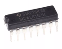
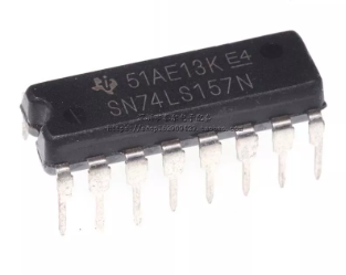
SN74LS157N (74LS157)
This content will be shared across all product pages.
Description:
The SN74LS157N IC contains four separate 2-input multiplexers, labeled as MUX1 to MUX4, with two data inputs (A and B), one select input (S), and one output (Y) per multiplexer. Multiplexers allow digital circuits to select between multiple input signals and choose one for output based on the control signal (select input). This IC is designed for high-speed operation and low power consumption, making it suitable for various digital logic applications requiring signal routing and selection.
Key Features:
- Quad 2-input multiplexers
- Low-power Schottky TTL technology
- Wide operating voltage range: 4.75V to 5.25V
- Typical propagation delay: 18 ns at VCC = 5V, CL = 15 pF
- High output drive capability: ±8 mA at VCC = 5V
- Direct compatibility with TTL input levels
- Schmitt-trigger inputs for improved noise immunity
- Package Type: 16-pin DIP (Dual In-line Package)
- Supply Voltage (VCC): 4.75V to 5.25V
- Input Voltage (VIN): 0V to VCC
- Output Voltage (VOUT): 0V to VCC
- Input High Voltage (VIH): 2V (min) at VCC = 5V
- Input Low Voltage (VIL): 0.8V (max) at VCC = 5V
- Output Current (IOH, IOL): ±8 mA (max)
- Quiescent Supply Current (ICC): 4 mA (max)
- Operating Temperature Range: 0°C to +70°C
- Data selectors and multiplexers
- Address decoding and signal routing
- Parallel-to-serial data conversion
- Bus interfacing and switching
- Digital signal processing and control systems
Technical Specifications:
- Logic Family: CMOS
- Number of Channels: 3
- Switch Configuration: Single-Pole Double-Throw (SPDT)
- Supply Voltage Range: 3V to 15V
- “ON” Resistance (R_ON): 125Ω typical at V_DD = 10V
- “OFF” Leakage Current (I_OFF): ±100pA typical at V_DD = 10V
- Control Input Voltage (V_IH): 0.7 V_DD min, 0.3 V_DD max
- Maximum Operating Frequency: 40 MHz at V_DD = 10V
Applications:
- Signal routing and switching
- Analog and digital multiplexing
- Audio and video signal processing
- Data acquisition systems
- Test equipment