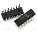
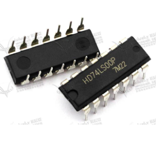
HD74LS00P (74LS00) Gate and Inverter
This content will be shared across all product pages.
Description:
The HD74LS00P is a high-speed, low-power Quad 2-input NAND gate integrated circuit. It features four independent NAND gates with two inputs each, capable of accepting standard TTL input levels and providing TTL compatible output levels. Each gate performs the Boolean function Y = A * B (Y = A AND B), where A and B are the inputs and Y is the output.
Key Features:
- Quad 2-input NAND gates in a single package
- High-speed operation: typically 12 ns propagation delay at VCC = 5V
- Low power consumption: typically ICC = 1.6 mA at VCC = 5V
- Wide operating voltage range: 4.75V to 5.25V
- TTL compatible inputs and outputs
- Direct interface with microprocessors and logic circuits
- High fan-out capability: can drive TTL or CMOS loads
- Package Type: 14-pin DIP (Dual In-line Package)
- Supply Voltage (VCC): 4.75V to 5.25V
- Input Voltage (VIN): 0V to VCC
- Output Voltage (VOUT): 0V to VCC
- Input High Voltage (VIH): 2V (min) at VCC = 5V
- Input Low Voltage (VIL): 0.8V (max) at VCC = 5V
- Output Current (IOH, IOL): ±8 mA (max)
- Quiescent Supply Current (ICC): 1.6 mA (typical) at VCC = 5V
- Operating Temperature Range: 0°C to +70°C
- General-purpose logic functions
- Digital arithmetic and data processing
- Clock generation and synchronization circuits
- Address decoding in microprocessor systems
- Interface logic in computer peripherals
Technical Specifications:
- Logic Family: CMOS
- Number of Channels: 3
- Switch Configuration: Single-Pole Double-Throw (SPDT)
- Supply Voltage Range: 3V to 15V
- “ON” Resistance (R_ON): 125Ω typical at V_DD = 10V
- “OFF” Leakage Current (I_OFF): ±100pA typical at V_DD = 10V
- Control Input Voltage (V_IH): 0.7 V_DD min, 0.3 V_DD max
- Maximum Operating Frequency: 40 MHz at V_DD = 10V
Applications:
- Signal routing and switching
- Analog and digital multiplexing
- Audio and video signal processing
- Data acquisition systems
- Test equipment