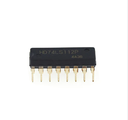
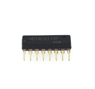
HD74LS112P (74LS112)
This content will be shared across all product pages.
Description:
The HD74LS112P is a dual J-K flip-flop integrated circuit designed for use in digital logic applications. It features two independent J-K flip-flops, each capable of toggling its output based on the clock input (CLK), J (set) input, and K (reset) input signals. These flip-flops are edge-triggered and can operate in toggle mode (both J and K high), set mode (J high, K low), reset mode (J low, K high), or hold mode (both J and K low). The IC is commonly used for frequency division, counting, and sequential logic circuitry.
Key Features:
- Dual J-K flip-flop IC
- Edge-triggered for synchronous operation
- Toggle, set, reset, and hold modes
- Wide operating voltage range: typically 4.75V to 5.25V
- Low power consumption
- Fast propagation delay: typically 14 ns at VCC = 5V
- TTL compatible inputs and outputs
- Package Type: 16-pin DIP (Dual In-line Package)
- Supply Voltage (VCC): 4.75V to 5.25V
- Input Voltage (VIN): 0V to VCC
- Output Voltage (VOUT): 0V to VCC
- Input High Voltage (VIH): 2V (min) at VCC = 5V
- Input Low Voltage (VIL): 0.8V (max) at VCC = 5V
- Output Current (IOH, IOL): ±8 mA (max)
- Quiescent Supply Current (ICC): 4 mA (typical) at VCC = 5V
- Operating Temperature Range: 0°C to +70°C
- Frequency division and counting circuits
- Sequential logic circuits
- Control and timing applications in microprocessor systems
- Clock signal generation and synchronization
Technical Specifications:
- Logic Family: CMOS
- Number of Channels: 3
- Switch Configuration: Single-Pole Double-Throw (SPDT)
- Supply Voltage Range: 3V to 15V
- “ON” Resistance (R_ON): 125Ω typical at V_DD = 10V
- “OFF” Leakage Current (I_OFF): ±100pA typical at V_DD = 10V
- Control Input Voltage (V_IH): 0.7 V_DD min, 0.3 V_DD max
- Maximum Operating Frequency: 40 MHz at V_DD = 10V
Applications:
- Signal routing and switching
- Analog and digital multiplexing
- Audio and video signal processing
- Data acquisition systems
- Test equipment