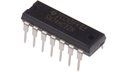

SN74HC32N (74HC32) Logic Gate/Inverter
This content will be shared across all product pages.
Description:
The SN74HC32N integrates four independent 2-input OR gates in a single package. Each OR gate accepts two binary inputs and outputs a high signal (logic 1) if at least one of its inputs is high. It operates at high speed and is compatible with TTL (Transistor-Transistor Logic) inputs, making it versatile for use in a wide range of digital logic applications.
Key Features:
- Quad 2-input OR gates
- High-speed CMOS technology
- Low power consumption
- Wide operating voltage range: 2V to 6V
- Typical propagation delay: 10 ns at VCC = 5V, CL = 15 pF
- High output drive capability: ±5.2 mA at VCC = 5V
- Balanced propagation delays
- Direct compatibility with TTL input levels
- Package Type: 14-pin DIP (Dual In-line Package)
- Supply Voltage (VCC): 2V to 6V
- Input Voltage (VIN): 0V to VCC
- Output Voltage (VOUT): 0V to VCC
- Input High Voltage (VIH): 3.5V (min) at VCC = 4.5V
- Input Low Voltage (VIL): 1.5V (max) at VCC = 4.5V
- Output Current (IO): ±5.2 mA (max)
- Quiescent Supply Current (ICC): 1 µA (max)
- Operating Temperature Range: -40°C to +85°C
- Digital logic circuits
- Microcontroller interfacing
- Arithmetic and logic operations
- Signal gating and switching
- Address decoding
Technical Specifications:
- Logic Family: CMOS
- Number of Channels: 3
- Switch Configuration: Single-Pole Double-Throw (SPDT)
- Supply Voltage Range: 3V to 15V
- “ON” Resistance (R_ON): 125Ω typical at V_DD = 10V
- “OFF” Leakage Current (I_OFF): ±100pA typical at V_DD = 10V
- Control Input Voltage (V_IH): 0.7 V_DD min, 0.3 V_DD max
- Maximum Operating Frequency: 40 MHz at V_DD = 10V
Applications:
- Signal routing and switching
- Analog and digital multiplexing
- Audio and video signal processing
- Data acquisition systems
- Test equipment