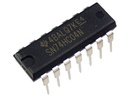
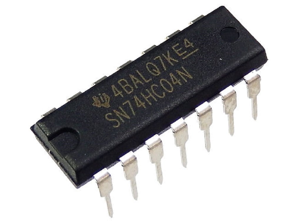
SN74HC04N (74HC04) Logic chip
This content will be shared across all product pages.
Description:
The SN74HC04N IC contains six individual inverters, labeled as INV1 to INV6, with one input (A) and one output (Y) per inverter. Inverters are fundamental logic gates that complement the input signal, producing the opposite logic state at the output. This IC is designed for high-speed operation and low power consumption, making it suitable for various digital logic applications requiring signal inversion.
Key Features:
- Hex inverter gates
- High-speed CMOS technology
- Low power consumption
- Wide operating voltage range: 2V to 6V
- Typical propagation delay: 9 ns at VCC = 5V, CL = 15 pF
- High output drive capability: ±5.2 mA at VCC = 5V
- Direct compatibility with TTL input levels
- Package Type: 14-pin DIP (Dual In-line Package)
- Supply Voltage (VCC): 2V to 6V
- Input Voltage (VIN): 0V to VCC
- Output Voltage (VOUT): 0V to VCC
- Input High Voltage (VIH): 3.15V (min) at VCC = 6V
- Input Low Voltage (VIL): 1.35V (max) at VCC = 6V
- Output Current (IO): ±5.2 mA (max)
- Quiescent Supply Current (ICC): 1 µA (max)
- Operating Temperature Range: -55°C to +125°C
- Signal inversion in digital circuits
- Buffering and signal conditioning
- Clock generation and distribution
- Pulse shaping and waveform generation
- Logic level conversion between different voltage standards
Technical Specifications:
- Logic Family: CMOS
- Number of Channels: 3
- Switch Configuration: Single-Pole Double-Throw (SPDT)
- Supply Voltage Range: 3V to 15V
- “ON” Resistance (R_ON): 125Ω typical at V_DD = 10V
- “OFF” Leakage Current (I_OFF): ±100pA typical at V_DD = 10V
- Control Input Voltage (V_IH): 0.7 V_DD min, 0.3 V_DD max
- Maximum Operating Frequency: 40 MHz at V_DD = 10V
Applications:
- Signal routing and switching
- Analog and digital multiplexing
- Audio and video signal processing
- Data acquisition systems
- Test equipment