
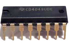
CD4049
This content will be shared across all product pages.
The CD4049 is a hex inverting buffer/converter IC that belongs to the CD4000 series of CMOS logic devices. It consists of six independent high-voltage, high-current buffer/inverter circuits. Each circuit can be used as a buffer with a high-impedance input and a low-impedance output or as an inverter with a Schmitt trigger action on the input.
Key Features:
- Hex inverting buffers
- Wide supply voltage range
- High noise immunity
- Low power consumption
- Buffered inputs and outputs
- Symmetrical output characteristics
- Logic Family: CMOS
- Number of Buffers/Inverters: 6
- Supply Voltage Range: 3V to 18V
- High-Level Output Voltage (V_OH): 14V min at V_DD = 10V
- Low-Level Output Voltage (V_OL): 0.1V max at V_DD = 10V
- High-Level Input Voltage (V_IH): 3.5V min at V_DD = 5V, 7V min at V_DD = 10V
- Low-Level Input Voltage (V_IL): 1.5V max at V_DD = 5V, 3.5V max at V_DD = 10V
- Propagation Delay Time: 60ns max at V_DD = 15V, C_L = 50pF
- Signal processing
- Data transmission
- Voltage level shifting
- Logic level conversion
- Pulse and waveform generation
Technical Specifications:
- Logic Family: CMOS
- Number of Channels: 3
- Switch Configuration: Single-Pole Double-Throw (SPDT)
- Supply Voltage Range: 3V to 15V
- “ON” Resistance (R_ON): 125Ω typical at V_DD = 10V
- “OFF” Leakage Current (I_OFF): ±100pA typical at V_DD = 10V
- Control Input Voltage (V_IH): 0.7 V_DD min, 0.3 V_DD max
- Maximum Operating Frequency: 40 MHz at V_DD = 10V
Applications:
- Signal routing and switching
- Analog and digital multiplexing
- Audio and video signal processing
- Data acquisition systems
- Test equipment