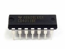
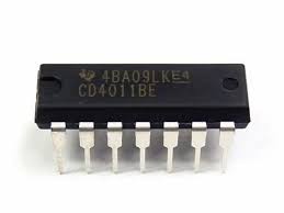
CD4011
This content will be shared across all product pages.
The CD4011 is a quad 2-input NAND gate IC from the CD4000 series of CMOS logic devices. It consists of four independent NAND gates, each with two inputs, that perform the logical NAND function. This IC is designed for use in a wide range of digital applications, including logic gate functions, signal gating, and data processing. The CD4011 is known for its high noise immunity, low power consumption, and wide operating voltage range.
Key Features:
- Quad 2-input NAND gates
- High noise immunity
- Low power consumption
- Wide supply voltage range
- Standardized, symmetrical output characteristics
- Buffered inputs and outputs
- Capable of driving two low-power TTL loads or one low-power Schottky load over the rated temperature range
- Logic Family: CMOS
- Number of Gates: 4
- Number of Inputs per Gate: 2
- Supply Voltage Range: 3V to 15V
- High-Level Output Voltage (V_OH): 2.9V min at V_DD = 5V, 4.95V min at V_DD = 10V
- Low-Level Output Voltage (V_OL): 0.1V max at V_DD = 5V, 0.05V max at V_DD = 10V
- High-Level Input Voltage (V_IH): 3.5V min at V_DD = 5V, 7V min at V_DD = 10V
- Low-Level Input Voltage (V_IL): 1.5V max at V_DD = 5V, 3V max at V_DD = 10V
- Propagation Delay Time: 200ns max at V_DD = 10V, C_L = 50pF
- Operating Temperature Range: -55°C to +125°C
- Package Types: PDIP, SOIC, TSSOP
- Logic gate functions
- Signal gating
- Data processing
- Control systems
- Digital electronics
Technical Specifications:
- Logic Family: CMOS
- Number of Channels: 3
- Switch Configuration: Single-Pole Double-Throw (SPDT)
- Supply Voltage Range: 3V to 15V
- “ON” Resistance (R_ON): 125Ω typical at V_DD = 10V
- “OFF” Leakage Current (I_OFF): ±100pA typical at V_DD = 10V
- Control Input Voltage (V_IH): 0.7 V_DD min, 0.3 V_DD max
- Maximum Operating Frequency: 40 MHz at V_DD = 10V
Applications:
- Signal routing and switching
- Analog and digital multiplexing
- Audio and video signal processing
- Data acquisition systems
- Test equipment