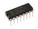
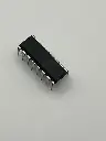

Description
The 74HC595 is an 8-bit serial-in, parallel-out shift register with an 8-bit storage register. The device features a serial data input (DS), eight parallel data outputs (Q0-Q7), and a serial output for cascading (Q7'). It is commonly used to expand the number of I/O pins available on a microcontroller, enabling control of multiple outputs with a few pins.
Key Features:
- 8-bit serial-in, parallel-out shift register
- 8-bit storage register with tri-state outputs
- Serial input (DS) and serial output for cascading (Q7')
- Three-state outputs (Q0-Q7)
- Low power consumption
- High-speed operation
- Cascadable with multiple 74HC595 ICs
- Operating Voltage: 2V to 6V
- Maximum Clock Frequency: 100 MHz (at Vcc = 4.5V to 5.5V)
- Current Consumption: 80 μA (maximum, at Vcc = 6V)
- Output Current per Pin: 35 mA (maximum)
- Total Current through Vcc/GND: 70 mA (maximum)
- Propagation Delay Time: 23 ns (at Vcc = 5V)
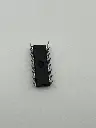
- Package Types: 16-pin PDIP, SOIC, TSSOP
- Operating Temperature Range: -40°C to +125°C
- LED displays
- Keypad interfaces
- Data acquisition systems
- Digital signal processing
- Memory addressing
- Control systems
- Connection:
- Connect the Vcc pin to a 5V power supply (or appropriate voltage within the operating range).
- Connect the GND pin to ground.
- Connect the serial data input (DS) to the microcontroller’s data output pin.
- Connect the clock input (SH_CP) and latch input (ST_CP) to the microcontroller’s clock and latch control pins.
- Connect the parallel outputs (Q0-Q7) to the desired peripheral devices.
- Use the serial output (Q7') to cascade additional 74HC595 shift registers if needed.
- Operation:
- Send serial data to the DS pin while providing clock pulses to SH_CP.
- Latch the data to the output pins by providing a pulse to the ST_CP pin.
- Control multiple 74HC595 ICs in series by connecting the Q7' of one to the DS of the next.
- Programming:
- Write code on the microcontroller to control the shift register.
- Shift in data bits and latch them to update the outputs as needed.
- Ensure the supply voltage does not exceed the maximum rated voltage to avoid damage to the IC.
- Handle the IC carefully to prevent damage from electrostatic discharge (ESD).
- Avoid exceeding the maximum current ratings to prevent overheating and damage.