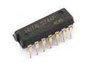
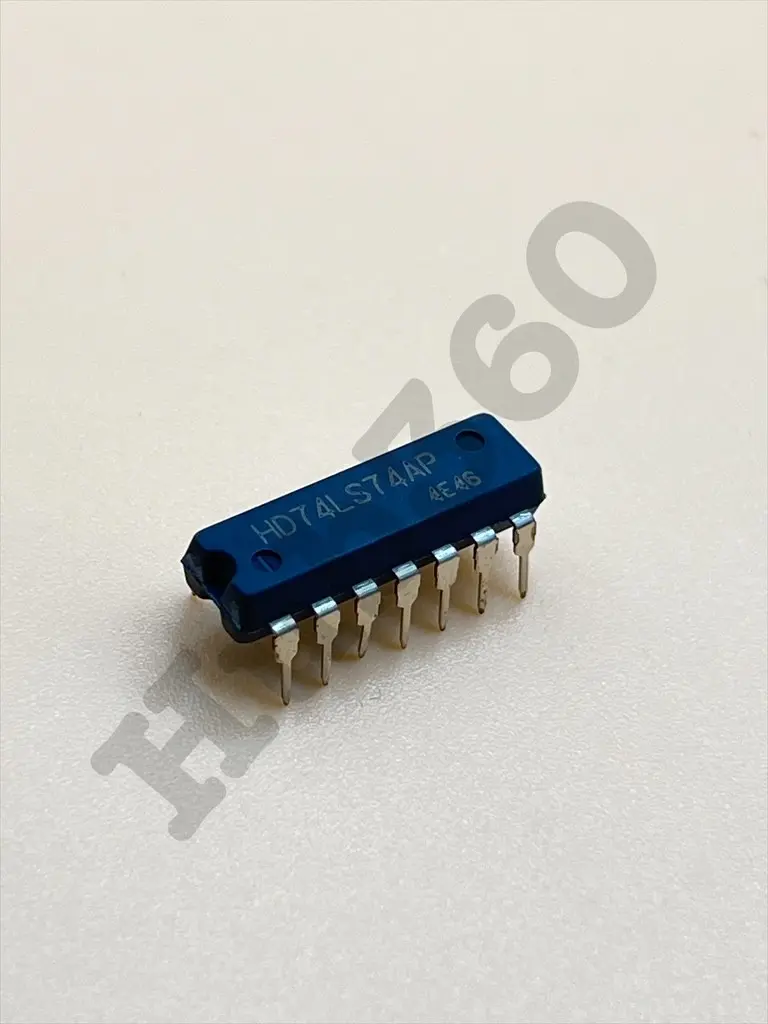
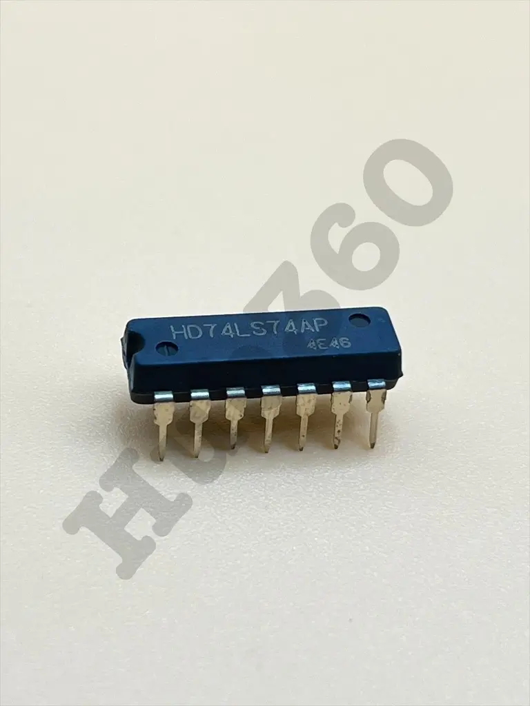

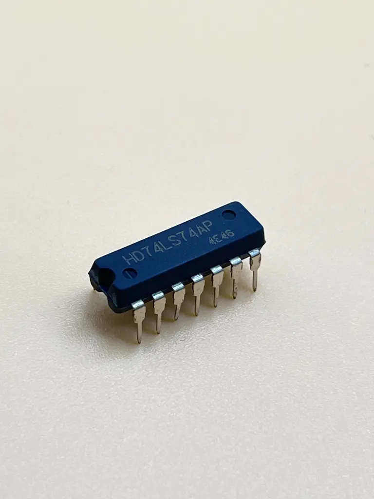
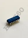
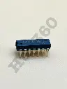

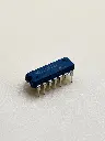
HD74LS74AP (74LS74) dual D trigger
Description:
The HD74LS74AP is a dual D-type flip-flop IC, consisting of two independent flip-flops each capable of storing a single bit of data. Each flip-flop has a data (D) input, a clock (CLK) input, and complementary outputs (Q and Q). The state of the flip-flop is determined by the data input at the moment of a clock signal transition (rising or falling edge, depending on the specific IC variant), allowing it to capture and retain digital data.
Key Features:
- Dual D-type flip-flops in a single package
- TTL compatible inputs and outputs
- Low power consumption
- Fast propagation delay: typically 15 ns at VCC = 5V
- Wide operating voltage range: 4.75V to 5.25V
- High noise immunity
- Package Type: 14-pin DIP (Dual In-line Package)
- Supply Voltage (VCC): 4.75V to 5.25V
- Input Voltage (VIN): 0V to VCC
- Output Voltage (VOUT): 0V to VCC
- Input High Voltage (VIH): 2V (min) at VCC = 5V
- Input Low Voltage (VIL): 0.8V (max) at VCC = 5V
- Output Current (IOH, IOL): ±8 mA (max)
- Quiescent Supply Current (ICC): 4 mA (typical) at VCC = 5V
- Operating Temperature Range: 0°C to +70°C
- Sequential logic circuits
- Frequency dividers and counters
- Memory addressing and data storage applications
- Clock and timing signal generation
- Control and interface circuits in digital electronics