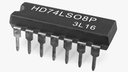
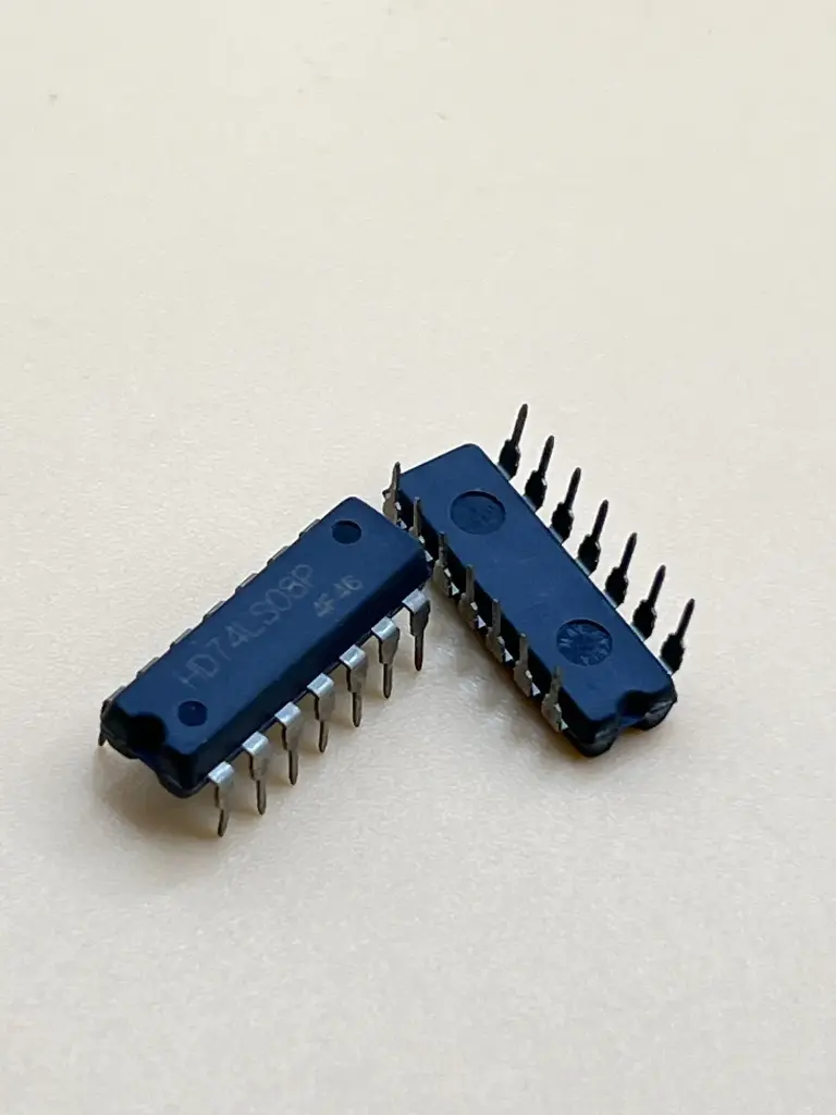

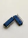
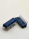
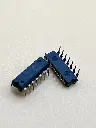
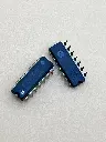
HD74LS08P (74LS08) Logic chip
Description:
The HD74LS08P is a quad 2-input AND gate IC, featuring four independent gates each with two inputs (A and B) and one output (Y). The output (Y) is high (logic 1) only when both inputs (A and B) are high (logic 1), otherwise, the output is low (logic 0). This IC is widely used in digital electronics for combining multiple logic signals, creating complex logical functions, and implementing various logic gates in electronic circuits.
Key Features:
- Quad 2-input AND gates in a single package
- TTL compatible inputs and outputs
- Low power consumption
- Fast propagation delay: typically 9 ns at VCC = 5V
- Wide operating voltage range: 4.75V to 5.25V
- High noise immunity
- Package Type: 14-pin DIP (Dual In-line Package)
- Supply Voltage (VCC): 4.75V to 5.25V
- Input Voltage (VIN): 0V to VCC
- Output Voltage (VOUT): 0V to VCC
- Input High Voltage (VIH): 2V (min) at VCC = 5V
- Input Low Voltage (VIL): 0.8V (max) at VCC = 5V
- Output Current (IOH, IOL): ±4 mA (max)
- Quiescent Supply Current (ICC): 4 mA (typical) at VCC = 5V
- Operating Temperature Range: 0°C to +70°C
- Logic gates and combinational logic circuits
- Signal processing and data manipulation
- Arithmetic circuits and data routing in microprocessor systems
- Clock generation and synchronization circuits
- Control and interface circuits in digital electronics