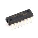

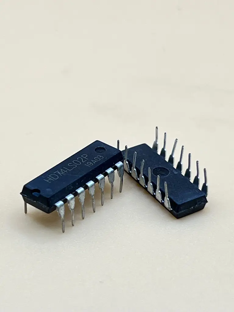

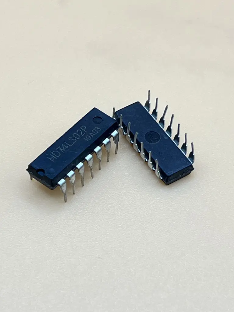
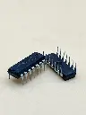
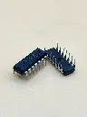
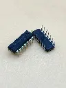
HD74LS02P (74LS02) Logic chip
Description:
The HD74LS02P is a quad 2-input NOR gate integrated circuit, designed to perform logical NOR operations on two inputs. Each gate within the IC has two inputs (A and B) and one output (Y), where the output is low (logic 0) only when both inputs are high (logic 1). This IC is widely used in digital electronics for various logic operations, including signal inversion, logic gates, and combinational logic circuits.
Key Features:
- Quad 2-input NOR gates in a single package
- TTL compatible inputs and outputs
- Low power consumption
- Fast propagation delay: typically 11 ns at VCC = 5V
- Wide operating voltage range: 4.75V to 5.25V
- High noise immunity
- Package Type: 14-pin DIP (Dual In-line Package)
- Supply Voltage (VCC): 4.75V to 5.25V
- Input Voltage (VIN): 0V to VCC
- Output Voltage (VOUT): 0V to VCC
- Input High Voltage (VIH): 2V (min) at VCC = 5V
- Input Low Voltage (VIL): 0.8V (max) at VCC = 5V
- Output Current (IOH, IOL): ±4 mA (max)
- Quiescent Supply Current (ICC): 4 mA (typical) at VCC = 5V
- Operating Temperature Range: 0°C to +70°C
- Logic gates and combinational logic circuits
- Signal inversion and pulse shaping
- Address decoding and data routing in microprocessor systems
- Clock generation and synchronization circuits
- Control and interface circuits in digital electronics